
Description
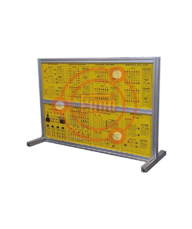
Digital Logic Lab Trainer
Specification (Category 1) :
Power Supply,Main Unit Dual DC Power Supply,
Voltage range : +5V/1.5A,-5V/0.3A,+-12V/0.3A,
With output overload protection,
Adjustable DC Power Supply,Voltage range : +1.5V ~ +15V,-
Max. current output : 0.5A,
With output overload protection,
Standard Frequency,Frequency : 1MHz,60Hz,1Hz,
Accuracy : +- 0.01% (1MHz),Fan out : 10 TTL load,
Clock Signal Generator,
Frequency : 1Hz ~ 1MHz (6 ranges),1Hz ~ 10Hz,10Hz ~
100Hz,100Hz ~ 1KHz,1KHz ~ 10KHz,10KHz ~
100KHz,100KHz ~ 1MHz,
Others Specification,
Fan out : 10 TTL load,Data Switch,
8-bit DIP switch x 2,16-bit TTL level output,
Toggle switch x 4,each with Debounce circuit,
Fan out : 10 TTL load,Pulser Switch,
-2 sets of independent control output,
-Each set with Q,Qft output,pulse width > 5ms,
-Each set of switch with Debounce circuit,
-Fan out : 10 TTL load,5 Universal counters,
Line Signal Generator,Frequency : 50Hz/60Hz,
Output voltage : 6Vrms,With overload protection,
Thumbwheel Switch : 2-digit,
BCD code output and common point input,
Logic Indicator: 16 sets of independent LED
indicates,high /low logic state,
Input Impedance : 100K ohms,
Digital Displays,2 sets of independent
7-segment LED display,With BCD,7-segment
decoder/driver and DP input,Input with 8-4-2-1,5mm
LED displays,InchLoInch and InchHiInch LED
display low/high logic state respectively,Speaker : 8
ohms,0.25W speaker with driver circuit,
Experiment Modules,
All 13 modules are equipped with an 8-bit DIP,switch for fault
simulation.,
Solutions for all fault test are listed in the,experiment manual for
userfts reference.,
2mm plugs and sockets are used throughout,the main unit and
all modules.,
Comprehensive experiment manual and instructorfts manual.
Module dimension: (255 x 165 x 30)mm.,
Connection plugs are used on the modules to, prevent accidental damages.,
Individual keeping case for each module,
List of Experiments :
Basic Logic Gates Experiments,
Introduction to logic gates and switches,
Logic gates circuits
Threshold voltage measurement
Voltage/current measurement
Basic logic gate transmission delay measurement
Measurement of basic logic gates characteristics
Interface between logic gates
Combinational Logic Circuits Experiments
NOR gate circuits
NAND gate circuit
XOR gate circuit
AND-OR-INVERT (AOI) gate circuit
Schmitt gate circuit
Open-collector gate circuits
Tristate gate circuits
Half-adder and full-adder circuits
Half-subtractor and fullsubtractor circuit
Arithmetic Logic Unit (ALU) circuit
Bit parity generator circuit
Encoder circuit
Decoder circuit
Multiplexer circuit
Demultiplexer circuit
Clock Generator Circuit Experiments
Constructing oscillator circuit with basic logic gates
Constructing oscillator circuit with schmitt gate
555 IC oscillator circuit
Monostable multivibrator circuits
Sequential Logic Circuit Experiments
Flip-flop circuits
J-K flip-flop circuits
Asynchronous binary up-counter
Asynchronous decade upcounter
Asynchronous divide-by-N up-counter
Asynchronous binary down-counter
Synchronous binary up-counter
Synchronous binary up/down counter
with single-chip microprocessor
Converter Circuit Experiment
Digital/Analog Converter (DAC) circuit
Unipolar DAC circuit
Bipolar DAC circuit
Analog/Digital Converter (ADC) circuit
8-bit converter circuit,
3 1/2 digit converter circuit,
Accessories:
Connecting Wire: 1 set
User Manual: 1 Nos
Standard Accessories
Others:
Country of Origin: China, Taiwan, Japan.
Manufacturing: Assemble in Bangladesh
Warranty: 1 Year
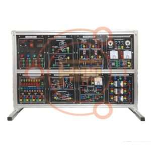
Specification (Category 2)
Main Unit
DC Power Supply
(1) Fixed DC power supply : +5V/2A, -5V/0.5A, +12V/2A
(2) With overload protection
Clock Generator
(1)Signal amplitude output : 3.3V
(2)With adjustable output frequency : square wave, 1Hz ~ 1MHz, 6 range
(3)Frequency display :4-digit, 7-segment LED
Logic Level Switch : Toggle switches x 8, 3.3V output
Data Level Switch : 8-bit DIP switch x 2, 3.3V output
Pulse Signal Generator
(1) 2 sets of toggle switch with independent control output
(2) Each set with Q, Q’ output
(3) Pulse width > 5ms, each with Denounce circuit Logic Level Indicator
(1) 16-bit LED with driver and protection circuit
(2) Input Impedance : > 100K ohms
8 Channel Logic Signal Tracer
(1) 8 logic signal input :input impedance : ≥100K ohms , 3.3V input
(2) Fixed DC level shift for each channel
(3) Input signal attenuation ratio : 1/8
(4) Output signal : BNC or 2mm plug
(5) Oscilloscope SYNC. select : ALT/CHOP and scan-frequency adjustment
(6) The function can be used only with analog oscilloscope
7-segment LED display & frequency measurement 2 DIP switches select the function :
(1) 00 : Scanning display mode
a.Common anode for the control of 7-segments a ~ g
b.Scanning cathode for the control of 4-digit S0 ~ S3
(2) 01 : Independent display mode
a.Input 4-digit of data individually and decode the data at 7-segment display separately
b.Independent binary input and hexadecimal output
(3) 10 : Frequency counter for internal clock
a.Display the frequency of clock generator from main unit
b. Frequency range : 0.001KHz ~ 999.9KHz
(4) 11 : Frequency counter for external clock
a.Display the frequency of clock signal from external unit
b. Frequency range : 0.001KHz ~ 999.9KHz Rotary Encoder
Rotary encoder output : PA, PB and GND
signal, 3.3V output
Standard Signal Generator
5 sets of frequency : 20MHz, 1MHz, 10KHz, 100Hz, 1Hz
Experiment Modules
All built-in DC power socket module supply DC power from the main unit. Each module includes a CPLD chip to
implement all digital circuits shown on module panel.2mm sockets, bridge plugs, and cables are used throughout all modules so that students can easily create the circuits and compare different results in short time. With comprehensive experiment manual.
List of Experiments
Combinational Logic Circuit Experiment
(1) NOR gate circuit
(2) NAND gate circuit
(3) XOR gate circuit
a. Constructing XOR gate with NAND gate
b. The combination with basic gates
(4) AND-OR-INVERTER (A-O-I) gate circuit
(5) Comparator circuit
a. Comparator constructed with basic logic gates
b. Comparator constructed with TTL IC
(6) Schmitt gate circuit
(7) Open-collector gate circuit
a. High voltage/current circuit
b. Constructing an AND gate with open-collector gate
(8) Half-adder and full-adder circuit Construct HA with basic logic gates
(9) Half-subtractor and full-subtractor circuit Subtractor circuit constructed with basic logic gates
(10) Bit parity generator circuit Bit parity generator constructed with XOR gates
(11) Constructing a 4-to-10 decoder with TTL IC
(12) The switch characteristics of TTL level conversion circuit
Arithmetical Logic/Tri-state & Code Converter Experiment
(1) CMOS FET tristate gate circuit
a. Truth table measurements
b. Constructing an AND gate with tristate gate
c. Bidirectional transmission circuit
(2) Half-adder and full-adder circuit
a. Full-adder circuit with IC
b. High-speed adder carry generator circuit
c. BCD code adder circuit
(3) Half-subtractor and full-subtractor circuit
Full-adder and inverter circuit
(4) Arithmetic Logic Unit (ALU) circuit
(5) Bit parity generator circuit Bit parity generator IC
(6) Hex to Dec/Dec to Hex digital conversion
a. 8-digit Dec-to-Hex conversion
b. 8-bit Hex-to-Dec conversion
Encoder, Decoder & Multiplexer Logic
Circuit Experiment
(1) Encoder circuit
a. Constructing a 4-to-2 encoder with basic gates
b. Constructing a 9-to-4 encoder with TTL IC
(2) Decoder circuit
a. Constructing a 2-to-4 decoder with basic gates
b. BCD-to-7-segment decoder
(3) Multiplexer circuit
a. Constructing a 2-to-1 multiplexer
b. Using multiplexers to create functions
c .Constructing a 8-to-1 multiplexer circuit with TTL IC
(4) Demultiplexer circuit
Constructing a 2-output demultiplexer with basic logic gates
(5) Digitally controlled analog multiplexer/demultiplexer circuit
(6) The switch characteristics of CMOS level conversion circuit
Flip-flop & Sequential Logic & Counter
Circuit Experiment
(1) Flip-flop circuits
a. Construct R-S flip-flop with basic logic gates
b. Construct D flip-flop with R-S flip-flops
c. Construct noise elimination circuit with R-S flip-flops
d. Construct J-K flip-flop with D flip-flops
e. The J-K flip-flop of delay and differential
f . Construct master-slave J-K flip-flops with dual R-S flip-flops
g. Construct shift register with D flip-flops
h. Preset left/right shift register
(2) J-K flip-flop counters
a. Asynchronous binary up counter
b. Asynchronous binary down counter
c. Asynchronous decade up counter
d. Synchronous binary counter
e. Synchronous binary up counter
f . Synchronous binary up/down counter
g. Johnson counter
h. Ring counter
Oscillator/Pulser ; Load ; Up/Down Counter
Circuit Experiment
(1) Constructing Random Access Memory (RAM) with D flip-flop
(7) Construct Non-retriggerable circuit with the specialized CMOS IC
(8) Construct retriggerable circuit with CMOS IC
(2) 64-bit Random Access Memory (RAM) circuit
(3) Erasable Programmable Read Only Memory (EPROM) circuit
(4) Asynchronous four-bit binary up counter (use of 7493 IC)
(5) Presetable binary up/down counter
(6) Presetable decimal up/down counter
(9) Construct a variable duty cycle oscillator circuit with dual monostablemultivibrators Memory, Matrix LED & DAC/ADC & MCU
Interface Circuit Experiment
(1) Electronic EPROM (EEPROM) circuit
(2) DAC0800 unipolar conversion circuit experiments
(3) Bipolar output conversion circuit
(4) ADC0804 8-bit SAC analog-to-digital converter experiment
(5) Constructing dynamic scanning counter with singlechip microprocessor Digital & Analog Timer, Pulse Generator
Circuit Experiment
(1) Constructing oscillator circuit with basic logic gates
a. Resistor-capacitor multivibrator
b. Resistor-capacitor crystal multivibrator
(2) Constructing oscillator circuit with schmitt gate
a. Resistor-capacitor oscillator
b. Variable duty cycle resistor-capacitor oscillator
(3) 555 IC oscillator circuit
a. 555 oscillator circuit
b. Voltage controlled oscillator circuit
(4) Monostable multi vibrator circuits
a. Low-speed monostable multi vibrator circuits
b. Monostable ON/OFF delay circuit
c. Monostable ON/OFF timer circuit
d. Construct monostablemultivibrator circuit with 555 IC
(5) Numerically-Controlled Oscillator (NCO)
signal generator
(6) Precise-frequency function generator
(7) Variable-duty-cycle NCO signal generator
(8) Variable-ON/OFF delay and difference control experiments
(9) Precise 15-bit symmetric/asymmetric
PWM generator
Ramp-compare/SAR/Dual-slope ADC
Experiment
(1) Simple R-2R unipolar output D/A converter experiments
(2) 8-bit digital-ramp A/D converter experiment
(3) 8-bit successive-approximation A/D converter experiment
(4) 8-bit dual-slope A/D converter experiment
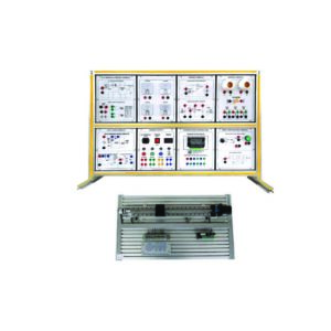
Keyboard & Display for Stepping Motor Position Control
(1) Stepper motor position/speed control experiment
Precise Digital Clock Timer
(1) Clock experiment
(2) Timer experiment
Universal CPLD & Breadboard Experiment
(1) Create block diagram/schematic file in QUARTUS
(2) 16-bit Hex counter
(3) 16-bit decimal counter
(4) 16-bit presetable decimal up/down counter
(5) 16-bit scanning controller for 7-segment display
(6) 16-bit up/down counter and its indication by a 7-segment display
(7) Electronic music box
(8) The traffic light with animation and time indication
Accessories:
Connecting Wire: 1 set
User Manual: 1 Nos
Standard Accessoriec
Others:
Country of Origin: China
Manufacturing: Assemble in Bangladesh
Warranty: 1 Year
Reviews
There are no reviews yet.